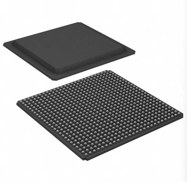
|
Manufacturer |
AMD
|
|
Manufacturer Product Number |
XCKU5P-2FFVB676I
|
|
Description |
IC FPGA 280 I/O 676FCBGA
|
|
Category
Integrated Circuits (ICs)
Embedded
FPGAs (Field Programmable Gate Array)
|
Total RAM Bits
41984000
|
|
Mfr
AMD
|
Number of I/O
280
|
|
Series
Kintex® UltraScale+™
|
Voltage – Supply
0.825V ~ 0.876V
|
|
Packaging
Tray
|
Mounting Type
Surface Mount
|
|
Part Status
Active
|
Operating Temperature
-40°C ~ 100°C (TJ)
|
|
DigiKey Programmable
Not Verified
|
Package / Case
676-BBGA, FCBGA
|
|
Number of LABs/CLBs
27120
|
Supplier Device Package
676-FCBGA (27×27)
|
|
Number of Logic Elements/Cells
474600
|
Base Product Number
XCKU5
|
Q1: What does the “I” and “-2” designation signify in XCKU5P-2FFVB676I? A: The “-2” represents the high-performance speed grade tier designed for faster logic toggle rates and lower routing delays. The “I” suffix denotes Industrial grade, certifying operation within a -40°C to +100°C thermal envelope.
Q2: What architecture node is used in the Kintex UltraScale+ XCKU5P series? A: The device is built on an advanced 16nm FinFET semiconductor manufacturing process, providing superior performance-per-watt efficiency compared to previous 28nm generations.